
Posted At: Jul 25, 2023 - 509 Views
ABSTRACT
V-Band millimeter-wave communication is an evolving technology for bandwidth-demanding 5G wireless applications. A high gain and linear wideband cascaded two-stage Low Noise Amplifier (LNA) operating at 52 to 60 GHz are presented in this paper. Proposed CMOS LNA circuit design yields a high gain of 30.7dB by forming a high Q-Network at the input terminal of the amplifying NMOS device and a source degenerative inductor. The noise Figure (NF) of the first cascaded stage is set as low to reduce the NF of the LNA as 3.92dB. Proper input and output impedance matching have performed to achieve the input return loss of -15.3dB and output return loss of -23.1dB. This circuit has a third-order input intercept point (IIP3) at -0.99dBm and requires 18.37 mW of power at 1.5V. The circuit was designed in Cadence Virtuoso 90nm technology and simulated using specter.
INTRODUCTION
Nowadays mobile phone technology advancement becomes more important due to the demands of users. Around 5 billion people are using mobile phones and 55% of connections are 3G/4G. Faster and reliable data connections for live video streaming becomes more important in the market. 3G and 4G operating bandwidth and spectrum are limited below 6GHz and occupied by many applications. 5G millimeter wave (30 to 300 GHz) networks are promising solutions for user requirements [1-3]. As per the result of the survey, the 60GHz band is recommended due to the high data rate and very high throughput. Apart from mobile data networks, application area like personal area networks (PAN), wireless backhauls, cloud computing and internet of Things (IoT) requires higher data rate with low area and cost constraints [4].
Several existing works have been carried out for these applications. Two-stage cascaded LNA operating at 55GHz has the NF of 3.6dB. Both stages have inductive source degeneration. This causes high power consumption and lower gain [5]. Transformer feedback neutralized LNA has advantages in terms of gain and power consumption with the cost of NF [6]. Our proposed work gives comparable gain and NF. Input and output matching networks, device parameters, LC components, and biasing points have designed to get effective results. This paper is organized as follows. Section 2 deals with the proposed cascaded LNA design and its relation between the design parameters. Section 3 gives an analysis of the responses of the LNA circuit. Section 4 concludes the proposed work.
PROPOSED CASCODED CMOS LNA DESIGN
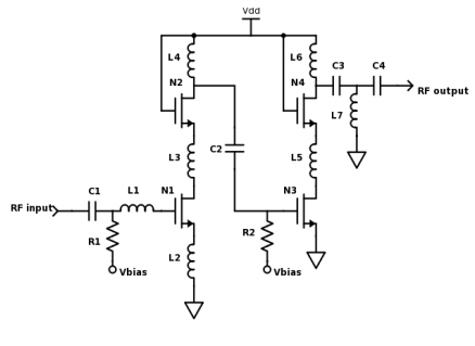
The proposed LNA should have an LC matching network, resistive biasing network, and cascaded two-stage amplifying network as shown in Fig.1. The cascaded structure is used to reduce power consumption. Wideband is achieved by stagger tuned two stages. Generally, NF of the LNA highly contributes to the total NF of the receiver side. That can be expressed from Friis formula as shown in Equ. (1),

The noise Figure of the receiver sideshows, a gain of the LNA has to be high enough to reduce the NF of the overall receiver. Based on this the design specifications have been considered as follows,

Design Parameters
LNA should be able to amplify the signal without adding much noise. For this purpose, the first stage of the LNA should have high gain and low NF. Total NF contributed by LNA can be expressed as in Equ. 2.

A schematic of the proposed LNA is shown in Fig. 2. The LNA circuit consists of a matching and amplifying network. The input matching network consists of C1, L1, L2, and Cgs1. Inductor L3 and L5 are used with Cgs2 and Cgs4 to tune each stage to their resonant frequencies. L6,7 and C3,4 are used at the output matching network. Capacitor C2 is used for coupling two stages. The source and load impedances have been considered as 50 ohm.
NF reduction using Lumped elements:
To improve the gain of the first stage LC tank circuits are formed at the gate and source terminals of the amplifying NMOS device N1. The Quality Factor (QF) of the LC network gets importance in the gain of the amplifier as in Equ. (3).

QF of the proposed first stage can be written in terms of LC and transconductance as in Equ. (4).

The quality factor of the LC series network is inversely proportional to the transconductance of the amplifying transistor. From Equ. 3 and 4 the gain of the first stage depends on LC values and the frequency, and independent of 𝑔𝑚1. Noise Figure (NF) of the first stage can be written as in Equ. 5. NF will be more or less equivalent to the effect of L1 and L2 as shown in Equ. 6.

The linearity of the LNA is determined by its IIP3 and P1dB points. Intermodulation linearity is represented as Third-order Input Intercept Point (IIP3) [7]. Total IIP3 of a two-stage LNA can be written as in Equ.7,

Overall IIP3 of the LNA is dominated by the last stage of the LNA. The final stage should be capable of handling large-signal coming from previous stages. The first stage of the LNA should have low NF and the last stage of the LNA should have high IIP3.
Linearity improvement by 𝑔𝑚 optimization:
The linearity of the second stage is optimized to improve the linearity of the LNA. IIP3 is inversely proportional to the gain and directly proportional to the transconductance of the amplifier. This can be referred from Equ. 7 and 8.

Source degeneration inductance is not used at the second stage. The bandwidth of the second stage has been tuned to be greater than the first stage to receive the signal from first stage, which causes the gain of the second stage to decrease. Q factor reduction and bandwidth improvement decreases the gain and improves the linearity.
𝑊3/𝐿3 ratio is increased as 40/0.1 instead of keeping the same ratio of the first stage, i.e) 𝑊1/𝐿1 = 30/0.1 . This device parameter adjustment increases the transconductance and thereby IIP3. Drain current 𝐼𝑑𝑠 depends on gate to source voltage 𝑉𝑔𝑠3. When 𝑉𝑔𝑠3 is increased, 𝐼𝑑𝑠 increases, and thereby transconductance and IIP3 increases. This is enabled by the bias voltage (Vbias = 0.4V) applied at the gate terminal of N3. Gate to source voltage at the second stage amplifying device (𝑉𝑔𝑠3 ) is kept as higher than 𝑉𝑔𝑠2 by using 𝑅1 > 𝑅2 to get high 𝑔𝑚3.

Impedance Matching
LC components are used to match the amplifier with the source impedance of 50Ω. As shown in the schematic L1 and C1 are used in series to form a tank circuit at the input of the amplifying transistor N1; L2 and Cgs1 are used to form a tank circuit at the source terminal of N1. Both of these tank circuits are used for impedance matching network [8]. The impedance seen from the source terminal is as in Equ. (10),

𝑔𝑚𝐿2 and 𝐶 are getting important to determine the input impedance. 3dB bandwidth was considered to design the output impedance and designed to match the load impedance with low Q value. Inter stage impedance is matched using L4 and C2 elements. Load impedance of 50Ω is matched using T network formed my 𝐿6,7 and 𝐶3,4
RESULTS AND ANALYSIS
Stability consideration According to rollet stability factor, 𝐾 should be greater than one, and stability parameter |∆| should be less than one for a system to be unconditionally stable. Equ. (11) and (12) are used for the calculation.

Where, 𝑆11- Input reflection coefficient, 𝑆12- Inverse gain, 𝑆21- Forward gain, 𝑆22- Output reflection coefficient. Figure 3 shows the input return loss is lower than -10dB at frequencies between 55 to 60 GHz.

Inverse gain (S12) is found as -49dB to -41dB at 52 to 60 GHz. Particularly at the desired frequency of 56 GHz, the inversion gain is -32.66dB as shown in Fig.4.
Forward gain is an important parameter that has an influence on the power gain and voltage gain of the LNA. In our targeted band of frequency 52 to 60 GHz, S21 is obtained as 14dB to 18dB as in Fig. 5. Peak forward gain of 28.85dB is available at 56GHz


Figure of Merit is the normalized parameter which is used to keep trade-off between the parameters of a LNA to get better efficiency based on specification. 𝐹𝑜𝑀 of the wideband LNA can be calculated from maximum gain, bandwidth, NF, and power consumption. Since the proposed work is compared with the systems designed for different center frequencies at different technology node, the parameters like channel length, operating frequency, and the supply voltage are considered for 𝐹𝑜𝑀calculation and comparable results are achieved as in Table 1.
CONCLUSION
This paper presents two-stage cascaded LNA for 52 GHz to 60 GHz V-Band application. The proposed LNA design gives better results compared with existing work. Matching network components and biasing points were designed for obtaining better results at 56 GHz frequency. Gain and NF have been improved as 30.7dB and 3.92dB. Input return loss and output return loss are less than -15dB. This CMOS LNA has improved the linearity by means of -0.99dBm of IIP3, -14.84dBm of OIP3, and P1dB of -1.46dBm. Also, Figure of Merit is calculated as 34.6 and that is comparable with other results. Power consumption can be reduced in future work.
REFERENCES
[1]. “5G Spectrum – Public Policy Position”, GSMA, London, UK, November 2016
[2]. Qian Liu, Xiaochuan Shi, Xu Wang, and Jia Li, “5g development in China: From policy strategy to user-oriented architecture”, January 2017
[3]. Hu Wang, “5g Vision, Characteristics and Requirements”, GSA Spectrum Group, June 2016
[4]. David Fritsche, Gregor Tretter, Corrado Carta,, and Frank Ellinger, “Millimeter-Wave Low-Noise Amplifier Design in 28-nm Low-Power Digital CMOS” IEEE Transactions on Microwave Theory and Techniques, Vol. 63, No. 6, June 2015
[5] H. Gao, et al , “A 48–61 GHz LNA in 40-nm CMOS with 3.6 dB minimum NF © employing metal slotting method,” IEEE Radio Frequency Intergrated Circuits Symposium, Vol.14, No.5,pp 154–157 March 2016.
[6] K. J. Kim, et al ,“ A 60 GHz CMOS gain-boosted LNA with transformer feedbacked neutraliser,”IEEE Electron. Lett. 51 (2015) 1461 (DOI: 10.1049/el.2015. 0336). Vol. 51 No. 18 pp. 1461–1462.
[7]. Hooman Rashtian, Shahriar Mirabbasi, Thierry Taris, Yann Deval, Jean-Baptiste Begueret, “A 4-stage 60-GHz low-noise amplifier in 65-nm CMOS with body biasing to control gain, linearity, and input matching”, Analog Integr Circ Sig Process, (Springer), 2012, Issue. 73, pp.757-768
[8]. Sunwoo Kong, Hui Dong Lee, Moon-Sik Lee and Bonghyuk Park, “A V-Band Current-Reused LNA with a DoubleTransformer-Coupling Technique”, IEEE Microwave and Wireless Components Letters, Volume: 26, Issue: 11, Nov. 2016, pp. 942-944
[9] Yiming Yu ,“A 54.4-90 GHZ Low –Noise Amplifier in 65- nm CMOS ,” IEEE Journals of solid state circuits ,vol. 99 ,no.pp. 1-13 ,August 2017.
[10] F. Meng, et al , “A compact 57–67 GHz bidirectional LNAPA in 65-nm CMOS technology,” IEEE Microw. Wireless Compon. Lett. 26 (2016) vol.26, no.8. August 2016.
[11] Yen-chung chiang ,“ A Low Noise Amplifier with coupled matching structure for V –Band Applicatins,” IEEE International Symposium on Radio Frequency Intergrated technology. vol. pp.133-135 August 2015.